01 Jun Explore the opportunities of the new LabRAM Odyssey Semiconductor
Posted at 10:44h
in News
Groot-Ammers | June 1st, 2023
The HORIBA LabRAM Odyssey Semiconductor aims at giving valuable insights into the properties of materials and devices, thereby serving semiconductor, data storage, LED, photovoltaic and other related nanoelectronics industry R&Ds.
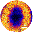
2D materials
- Raman microscopy is the technique of choice for the characterization of graphene and other 2D materials. The LabRAM Odyssey Semiconductor enables wafer uniformity assessment of layer thickness and crystalline quality, as well as defect review, to address the challenge of scaling up.
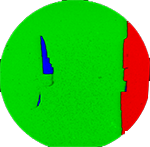
Group IV Semiconductors
- The unique sensitivity of Raman microscopy to mechanical stress, chemical composition, doping and crystallography combined with its non-destructive character and exceptionally fast time-to-result, has made the LabRAM Odyssey an ideal tool for the characterization of the historically established group IV materials.
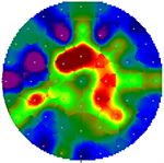
Compound Semiconductors
- The compound semiconductors’ (III-V, SiC, and III-nitrides) rapid growth linked to the emergence of IoT and power devices motivates development of quasi 2D or ultra-thin films and integration with Si technology. Raman and photoluminescence microscopes are essential tools for the deposition of prime grade materials. The LabRAM Odyssey Semiconductor is capable of both checking the quality uniformity over the entire wafer surface and highlighting/analyzing the presence of defects.
Keep me updated!
Just enter your name and email and don't miss out on all innovative technologies in the world of surface analysis.